A mere quarter after launching the impressive TITAN X, NVIDIA is launching another powerful flagship graphics card GPU from its silo leveraging the technology and design from the TITAN X GPU to deliver and maintain flagship performance. Enthusiasts wanted TITAN X performance at a lower price and we have got it. In our testing, 980 Ti reference card matched and even beat TITAN X in some benchmarks, yet significantly , faster add-in-board partner custom overclocked 980 Ti are coming. All of which posing a significant thread to AMD’s plans of Fast and ‘Furious’ domination of the high end graphics segment.
NVIDIA’s GTX 980 Ti is the fastest graphics card we have tested. Combined with support for DirectX 12 Feature Level 1 and updates to G-SYNC and Gameworks to optimize the VR experience, the standard has been set for AMD’s upcoming GPU release.
Due to an extremely tight review deadline, we present overall benchmarks in our launch review. Additional Benchmarks, Third Party Board specs and pricing and hardware tear-down/analysis may be added and updated to this review in the days after publishing.
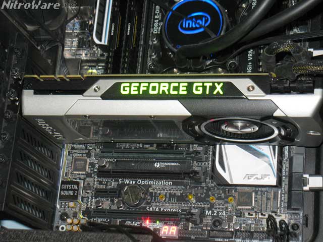
Introducing GTX 980 Ti
 Enthusiasts out there anticipating the GTX 980 Ti are likely familiar enough with 2nd generation Maxwell GPUs and want to skip straight to the point, great so do we. But first, before we get to the benchmarks:
980 Ti takes the ‘full’ TITAN X implementation of NVIDIA’s GM200 GPU and disables 2 of the 24 SMX units giving us 2816 shader cores, 176 Texturing Units and 96 ROPS, essentially a cut down version of TITAN X without any significant performance penalties or caveats, other than reduced texturing throughput and computational performance.

Now about those disabled units… Noting the general arrangement of the logical and physical processing units on the GPU as we have described, NVIDIA have elected to disable only half of a processing cluster which is the smallest usable logical unit of the GPU. Disabling half of the cluster preserves the Rasterization units and memory controllers.
In the official and simplified marketing diagram for the GPU which we annotated above, one may notice the excess ROPS and Raster Engine once the two SMM units are disabled.
Does this mean that these ROPS and Rasterizes while present are idle and not used/connected to any GPU cores? Not Necessarily.
What the diagram is missing is various crossbar buses which connect all the logical and compute units of the GPU together such as the SMMs, GPCs, the Cache and memory controllers.
Yes a fully populated Graphics Cluster with its 4 SMMs can make best use of its adjacent ROPS and rasterizers, but a less populated cluster can still use all the units via a crossbar bus at the expensive of some efficiency.
Under utilized ROPS and Rasterization Engine may sound like the situation with 970M where the partitioned memory is slower and not fully utilized but the difference with 980 Ti and GM200 is no memory controllers are crippled. All the hardware is present, except that some cores and texturing units are disabled. According to our testing we did not experience any performance regression compared to a TITAN X, especially at 4K Ultra Max Details.
We will still observe and report on the caveats of using this method (disabling SMMs) to produce different GPUs.
At 5.6 Tera-flops, 980 Ti is NVIDIA’s fastest consumer oriented GPU and now oddly enough, both its computing performance and texturing throughput match those of some third party editions of AMD’s Radeon R9 290X. With paper specs the same, it makes comparing efficiency of both cards, ie which is actually faster in game much more interesting.W
Since 980Ti does use the GM200 GPU from TITAN X, it also carries along the same PCB, therefore the memory system and importantly power supply topology. This product refresh mirrors what we saw from NVIDIA in 2012-2013 almost exactly. Early 2012 saw the GK104 powered GTX680 ship, it has a simplified onboard power supply which allowed for flexible customization by third party add in board partners and cost optimization. GTX 680 and 980 used high/low side MOSFET and driver sets while TITAN, 780/Ti, TITAN X and 980 Ti use fully integrated digital power chips which we described in our TITAN X review. AIB partners are not permitted to increase the video memory from 6GB.
Early 2013 brought us the first generation GTX TITAN built on GK110 with a premium heatsink-fan assembly and on-board power supply. Mid 2013 brought us the GTX 780 also with GK110 and the now iconic silver NVIDIA cooler and late 2013 brought the 780Ti.
The same cycle repeats itself for 2014-2015. late 2014 saw the launch of the cost optimized GTX 980 (albiet with the premium cooler unlike GTX 680) with GM204 core, followed up again by a refreshed TITAN X again fitted with a larger GM200 core. We now finally have the 980 Ti which ups the ante and provides a true flagship to the GPU stack. There actually is not much more headroom left for Maxwell GM200 series GPUs, which will have to battle AMD’s upcoming parts with high bandwidth memory and wait out the market until 2016’s ‘Pascal’ GeForce Refresh.
| Card | GTX 680 | GTX 780 Ti | GTX 980 | GTX TITAN X | GTX 980 Ti | R9 290X |
|---|---|---|---|---|---|---|
| Pixel Fillrate (GP/s) | 32.2 | 42 | 72 | 96.2 | 96 | 64 |
| Texture Fillrate (GT/s) | 128.8 | 210 | 144 | 192 | 176 | 176 |
| Memory Bandwidth (GB/s) | 192 | 336 | 224 | 337 | 337 | 320 |
| Single Precision Compute (GFLOPS) | 3090 | 5046 | 4612 | 6200 | 5632 | 5632 |
| Double Precision Compute (GFLOPS) | 195 | 210 | 144 | 192 | 176 | 704 |
| Single Precision Efficiency(GFLOPS/Watt) | 15.85 | 20.2 | 28 | 24.6 | 22.5 | 19.4 |
- CUDA/Shader core count between Kepler ‘SMX’ and Maxwell ‘SMM’ modules on the GPU should not be compared due to architectural differences.
- Dual GPU GTX TITAN Z board omitted for clarity, specs are slightly less than two TITAN Black
- Maxwell GM200 series retains 1/32 double precision performance of GeForce
- TFLOPS is calculated as 2x core count x clock speed. For Titan X NVIDIA took the Boost clock. 2x 3072 x 1089 = 6.63 TFLOPS which correlates to NVIDIA’s stated 7 TFLOPS as advertised, however we have used the base clock for our values, as for NVIDIA GPUs the base clock is guaranteed minimum.
GTX 960 and its GM206 GPU introduced an updated video processor which fully supported H265 HEVC video compression and decompression in hardware, however this updated unit didn’t make it into GM200 and neither TITAN X or 980 Ti have this enhanced NVENC video unit.

GTX 960 shipped with full DirectX12 branding on the box and simultaneously NVIDIA widely spoke of how GEFORCE was the preferred DirectX12 GPU for Microsoft as well as ISV demos. With WHQL drivers for Win 10 already published and basic DirectX12 evaluations already performed on Windows 10, with 60 days to go before the operating system’s release NVIDIA are now being very specific on which of their Geforce GPUs support which features and to drive the point home that they are fully DX12 compliant
During our briefing on GTX 980 Ti, Mobile G-SYNC and Gameworks VR we were informed that 2nd generation Maxwell supports the optional DirectX 12 Feature Level 1 while older GPUs such as Fermi would receive support through the Direct3D 12 API for common DirectX 12 software features as they lack the necessary hardware.