NVIDIA's tradition and legacy has been to always produce a compelling mid range GPU appealing to the 'sweet spot', that is the optimal performance/value offer to the large majority of semi-casual,budget concious PC gamers who would still want decent gaming performance. 2015 is no exception with the GTX 960 replacing the GTX 760 and delivering what NVIDIA has promised of the card, a cool, quiet, over-clockable and value for money card.
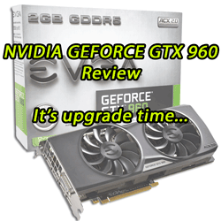
In this review we compare the GTX 960 (specifically EVGAs SSC model with ACX 2.0 cooling) to both MSI's GEFORCE GTX 760 HAWK and RADEON R9 270X HAWK, the 960's predecessors from 2013 as well as an overview at how the GTX 960 performs at 4K compared to its bigger brother GTX 980.
We were able to confirm GTX 960 offers more performance at lower power.
Background
Upon release of the GTX 980/970 in September 2014, NVIDIA did not initially replace the GTX 750/ti whose purpose in the product stack was for value for money efficient mid range gaming for casual gamers, below the GTX 760 being the mainstream performance offering. It was obvious that a 960 would eventually be released to deliver a top to bottom stack of cards based on the 2nd generation Maxwell GPU core once the GTX 980 launched, bringing with it all the benefits or of Maxwell GM200 core.
Both the 970/980 proved excellent performers (as they should be, being the Geforce top dogs), delivered good value per dollar, ran relatively cool and were over-clockable. This set the benchmark, no pun intended for any further refreshes and versions of GM200 based GPU cores that would turn up in future graphics cards.
Conveniently, GTX 960 is half a GTX 980 both on paper and physically which makes some comparisons easier. Its almost half the price too.
Enthusiasts often expect too much from unannounced products, and to determine what to expect we need to look at things logicically. When we have a stack of hardware products, in this instance microprocessor performance based such as a CPU or GPU
The majority of sales and shipments are typically the more affordable,value oriented cards what NVIDIA refers to as the 'sweet spot' of price and performance. Whether it was the GeForce 256 of 2000 or the GTX 980 of 2014, the high end cards are for those power users and enthusiasts who can afford them. The price-point of these cards has not changed much since the original GeForce as there has always been cheaper offerings for those more value oriented gamers and enthusiasts.
By course of NVIDIA nomenclature, the sweet spot cards have typically named as model 6 on the scale from 2 to 9, with 9 usually being a ultra or GPU card for the '1%' who must have the best of the best. 1 to 3 are entry for basic graphics and legacy games, 4 and 5 offer entry level performance, 6 offers mainstream performance for the budget concious enthusiast, 7 and 8 are high performance for enthusiasts and 9 is the ultra or dual GPU offering for the extreme enthusiast.
Considering programmable, DirectX 9 GPUs such as the 6600 GT, 7600 GT, 8600, 9600, 260, 460, 560ti, 660ti and 760 have sold well and delivered the value and performance enthusiasts expect. At the time of writing the GTX 460 despite being a 2010 release can still deliver playable frame rates with good visuals at 1080p providing the detail settings are optimised.
This time around NVIDIA hopes the GTX 960 continues the trend and is intended to be an upgrade path for these older GPUS, with improved paper specs while at the same time requiring minimal power.
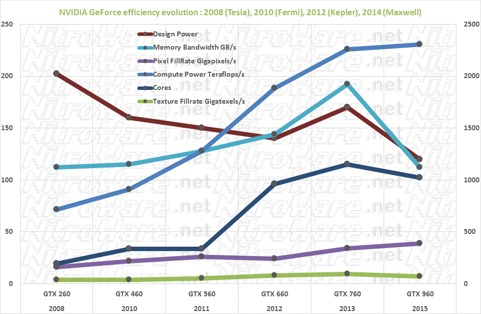
The GTX260 was one of the first mid GPUs that leveraged the design of its higher performing siblings models, utilising a large PCB, GPU die size and required two 6-pin connectors. This methodology of disabling cores and using a common PCB reduced time to market and offered increased performance at the expense of end user cost, power and heat. 460/560 continued this trend, while these parts specifically were OK compared to the 480/580 in efficiency, it wasn't until we saw the Kepler based GTX 660/660ti that signified a reversal of this trend with emphasis being placed on reducing cost, size, power.
Although 660/ti specifically needed 2 6-pin power plugs to work, many designs came on a shortened PCB to allow Add-In-Board makers to offer cheaper designs and for these cards to fit in a wider range of typical chassis. With Kepler in 2012, we finally saw a reversal of the ever increasing power budget and GTX 960 is the result of this reversal, with power requirements going full swing. Mainstream-Performance oriented GPU with a single power socket have been uncommon over the past few years.

We saw a reduction or stabilisation with TDPs for CPUs but the upward trend for GPUs was somewhat alarming especially to those keeping track of developments. For NVIDIA to improve their designs to such a degree and require significantly less power while still on the 28nm die process is an amazing feat.
We could have performed an 'upgrade' style test and article comparing GTX 460 and 960 but for this particular segment the 960 with its higher pixel and texture fillrates (ie how fast the GPU can render 3D graphics to the screen),similar memory bandwidth and reduced power requirements is just superior on paper, there's also the five plus years of development, a long time
Comparing against the previous generation GTX 760 and equivalent AMD Radeon which we did has its caveats too...
With Kepler based 600 series cards of 2012, we had a GTX 660 which was half a 680, a 'cut' die which is physically smaller and a GTX 660ti which offered higher performance and used the full GPU die from the GTX 680 with some Streaming Multiprocessor (abbreviated as SMX for Kepler, SMM for Maxwell) disabled to provide some differentiation.
For the 700 series update to Kepler, retail received the 1152 core GTX 760 and OEMs the 1344 core GTX 760 Ti, both based on the GK104 core and having half the core count of a GTX 780 and GTX TITAN respectively. The obfuscation of the 760 Ti is a little confusing but given the 700 is a refresh with higher performance the change in model line-up is not unexpected. The 760Ti may have been kept out of retail due to cost and cannibalisation concerns. 860 was skipped, being a Notebook GPU.
NVIDIA has been very careful to compare the 960 to the 660 (and 560/460) not the higher performance and cost Titanium editions, claiming 960 is 2X the power and the efficiency of the GTX 660 of 2012.
GTX 660 had 960 CUDA cores, 760 1152 and both 660ti/760 ti have 1344 of Kepler Generation. 960 has 1024 CUDA cores of Maxwell generation. Just on core count or design we cant compare directly as Maxwell is a re-architecture GPU, What about price? GTX 660 launched at US$229 and 760 at US $249, yet 960 at from US $199.
So comparing against the previous generation tells us if the manufacturer/designer's goals have been met and if a change in thinking delivers a better user experience, which may be at the expense of some overall performance yet at a gain of efficiency.
With a paper comparison against the most recent parts skewed, this leaves it up to benchmarks to see how much/if 960 is faster than a 760 and how much less power it uses. Even if 960 isn't faster or is even a little slower than 760, that's still a win as the card is cheaper new and consumes less power.
In some of our tests the Factory over clocked 960 was slower or the same as the factory over clocked 760 but considering we measured less idle and load power, GTX 960 is an example of where faster isn't necessary better !
The following table shows GeForce evolution and execution, we started with 200 'tesla' series, despite the 800 series (G80) having the first unified shader design. Even older chips such as NV40 and G70 had separate pixel and vertex shaders plus G80 based models do not line up with later generations easily.
| GeForce | Year | Codename | TDP | Cores | TMU | ROPS | Mem Bandwidth | Memory Width | Pixel Fillrate | Texel Fillrate | TFLOPS |
|---|---|---|---|---|---|---|---|---|---|---|---|
| GTX 260 | 2008 | GT200 | 202 | 192 | 64 | 28 | 112 GB/s | 448-bit | 16 GigaPixel/s | 37 GigaTexel/s | 715 |
| GTX 460 | 2010 | GF104 | 160 | 336 | 56 | 32 | 115 GB/s | 256-bit | 22 GigaPixel/s | 38 GigaTexel/s | 907 |
| GTX 560 | 2011 | GF114 | 150 | 336 | 56 | 32 | 128 GB/s | 256-bit | 26 GigaPixel/s | 50 GigaTexel/s | 1277 |
| GTX 660 | 2012 | GK106 | 140 | 960 | 80 | 24 | 144 GB/s | 192-bit | 24 GigaPixel/s | 79 GigaTexel/s | 1882 |
| GTX 760 | 2013 | GK104 | 170 | 1152 | 96 | 32 | 192 GB/s | 256-bit | 31 GigaPixel/s | 94 GigaTexel/s | 2258 |
| GTX 960 | 2015 | GM206 | 150 | 1024 | 64 | 32 | 112 GB/s | 128-bit | 39 GigaPixel/s | 72 GigaTexel/s | 2308 |
| Radeon | Year | Codename | TDP | Cores | TMU | ROPS | Mem Bandwidth | Memory Width | Pixel Fillrate | Texel Fillrate | TFLOPS |
|---|---|---|---|---|---|---|---|---|---|---|---|
| HD 7850 | 2012 | Pitcairn Pro | 130 | 1024 | 64 | 32 | 154 GB/S | 256-bit | 28 GigaPixel/s | 55 GigaTexel/s | 1761 |
| R9 270X | 2013 | Curacao XT | 180 | 1280 | 80 | 32 | 179 GB/s | 256-bit | 32 GigaPixel/s | 80 GigaTexel/s | 2688 |
| R9 285 | 2014 | Tonga Pro | 190 | 1792 | 112 | 32 | 176 GB/s | 256-bit | 29 GigaPixel/s | 103 GigaTexel/s | 3290 |
Source:Wikipedia, AMD, NVIDIA, and own sources. All cards 'reference'.
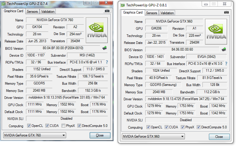
For this review, the MSI HAWK cards we compared our over clocked GTX960 to were also heavily over clocked, in the case of the of MSI GTX 760 HAWK, while its pixel fillrate is slightly less than 960, its texture and memory throughput are significantly faster. If GTX 960 can outperform this 760 then that is an accomplishment.
